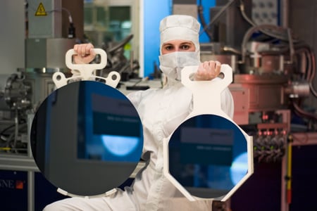
At SemiCon Technical Conference, 450mm Silicon Gets REAL!
If you have never worked in the semiconductor industry, much of what goes on seems like intentionally obfuscated jargon and black magic. And for many years it was – or at least it seemed to be – as empirical knowledge outstripped theoretical understanding, and yields were more a factor of skilled process engineers at the knobs than of robust and thoroughly understood processes running in statistical control. When I got involved in the semiconductor industry, wafer size was 100mm (4 inches) with a ‘flat’ along one or both edges, and a rather ‘generous’ edge exclusion area and ‘kerf’ between device…